
Foshan Fulan Laser Technology Co., Ltd.
National Hotline: 0757-29899345
Manager Wen: 18902563402
Fax: 0757-29899345
Business QQ: 2801827697
E-mail: china@fsfulan.com
Address: No.14, Leliu Port Intensive Industrial Zone, Shunde District, Foshan CityThe high-tech zone almond altar town, shunde, foshan city shun industry west road no. 15 cimc valley 20 9 / f, building B
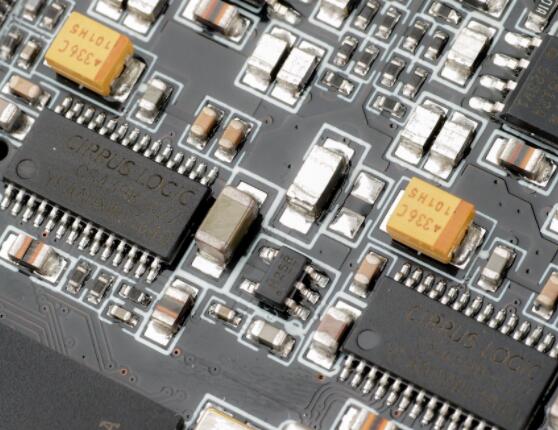
Chip is a general term for semiconductor component products. An integrated circuit consisting of a large number of transistors. Different chips have different integration scales, ranging from hundreds of millions to tens or hundreds of transistors.
(PS: Integrated circuit English: integrated circuit, abbreviated as IC; or microcircuit, microchip, wafer/chip.)
The chip naming method is generally: letter + number + letter, the letter in front is the abbreviation of the chip manufacturer or a certain chip series. The number in the middle is the functional model. Most of the following letters are package information. It depends on the information provided by the manufacturer to know what package the specific letter represents. A complete IC model generally identifies the manufacturer, device name, temperature class, package, speed, process structure, environmental protection, packaging, and version number.

There are many chip models and specifications. In order to quickly identify the brand or parameters and other information, we are bound to mark some graphic numbers or two-dimensional codes on the surface. At present, laser marking is the best choice. Advantages of laser marking: the marked mark is durable and anti-counterfeiting; non-contact processing; wide applicability; high engraving accuracy; low operating cost; high processing efficiency; simple operation; stable performance; environmental protection; strong flexibility , Can mark any content, and the content can be edited immediately; especially the marked pictures and texts are exquisite and beautiful, non-erasable, and will not be affected by environmental relations (touch, acid and reduced gas, high temperature, low temperature, etc.) or time. Fading, this can not only improve the quality of the product, but also play a role in preventing cross-products and counterfeiting. The most important thing is that laser marking will not damage the performance of the chip.
Recommended model: 3W UV laser marking machine
Because the laser wavelength of the ultraviolet laser marking machine is 355nm, the laser is a cold light source (so it is often called a cold light laser marking machine), the focusing spot is very small, and the processing heat affected zone is very small, and the thermal impact during marking is particularly small, so Super fine marking can be carried out.
The UV laser processing process is called the "photoetching" effect. The short-wavelength high-energy photons are processed by "cold" to directly destroy the chemical bonds of the atomic components of the material without generating heat. The processed material has smooth edges and extremely low limits. Carbonization. It solves the problem of insufficient marking and poor effect of many materials with fiber optic machine, green light machine, carbon dioxide machine and MOPA machine.
UV laser marking machine is mainly used in the high-end market of ultra-fine processing: marking of polymer materials and brittle materials; removal of metal or non-metal coatings; scribing of various materials and blind groove processing; new ultra-thin metal foil micro-holes Manufacturing; marking and scribing of flexible pcb boards; processing of micro-holes and blind holes of silicon wafers; drilling of glassware, etc.